Semiconductor wafer inspection using allPIXA wave and allPIXA evo
Mon, 2024-07-15
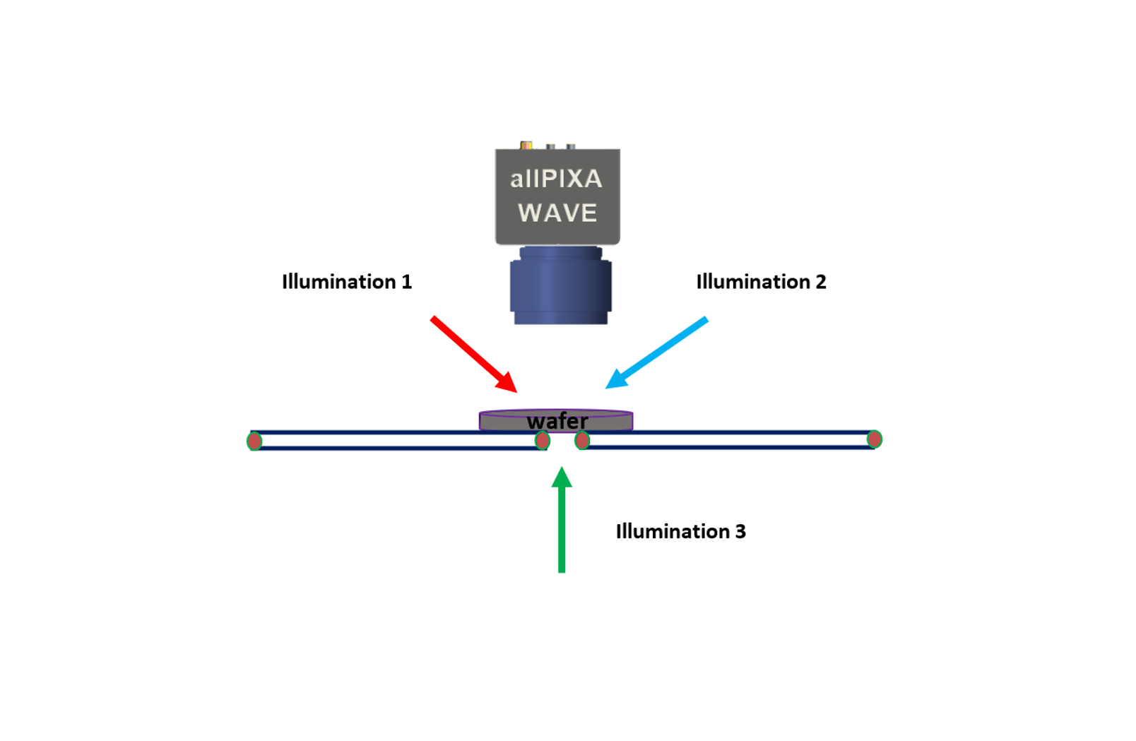
Capturing yield limiting defects is crucial for semiconductor wafer devices yield. Here we describe how semiconductor wafer manufacturing can take advantage of allPIXA wave ultra-high resolution 15,360 pixels and rich features to advantage of the in-line inspection systems.
Read the application note here.