News


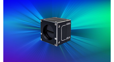
Introducing the allPIXA evo 32k Line Scan Camera
With the new allPIXA evo 32k, we’re excited to introduce our most advanced monochrome line scan camera, developed for inspection environments where micron accuracy and maximum throughput are equally critical.

allPIXA neo - the new multispectral camera with 4k and 6k resolution
allPIXA neo is the new multispectral camera series in the Chromasens allPIXA family.
With its small size and a quadlinear CMOS sensor, which in addition to RGB also creates a mono and NIR image in 4k and 6k resolution, this small power cube offers versatile possibilities for inspection tasks at high speed.

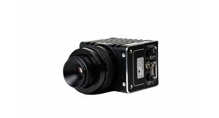


First Chromasens SWIR camera
The allPIXA SWIR is the first short-wave infrared (SWIR) line scan camera in Chromasens' allPIXA family.

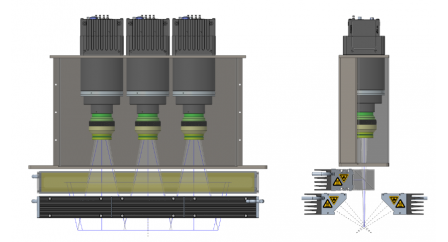
Technical Note - Semiconductor wafer inspection using allPIXA wave
Capturing yield limiting defects is crucial for semiconductor wafer devices yield. Here we describe how semiconductor wafer manufacturing can take advantage of its ultra-high resolution 15,360 pixels and rich features to advantage of in-line inspection systems allPIXA wave Trilinear color and mono TDI line scan camera.