Solutions for
Electronics & Semiconductor
Electronics & Semiconductor
For the inspection of electronic components (AOI, Automated Optical Inspection) high-resolution camera systems are indispensable nowadays. Whether for wafer production, semiconductor or PCB inspection, all components must be inspected to ensure the highest product quality and process reliability. Demanding applications include machine inspection in several stages of the manufacturing process, whereby the inspection is carried out in 2D and 3D using high-resolution camera systems.
Applications:
The most important requirements for cameras for semiconductor and electronics inspection:
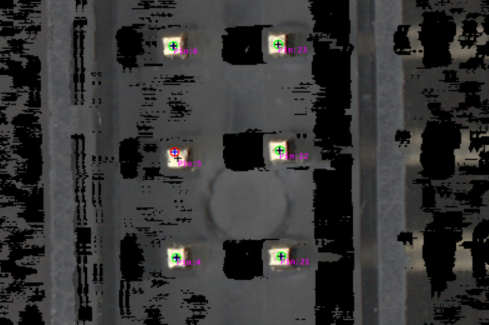
3D card of an electronic connector
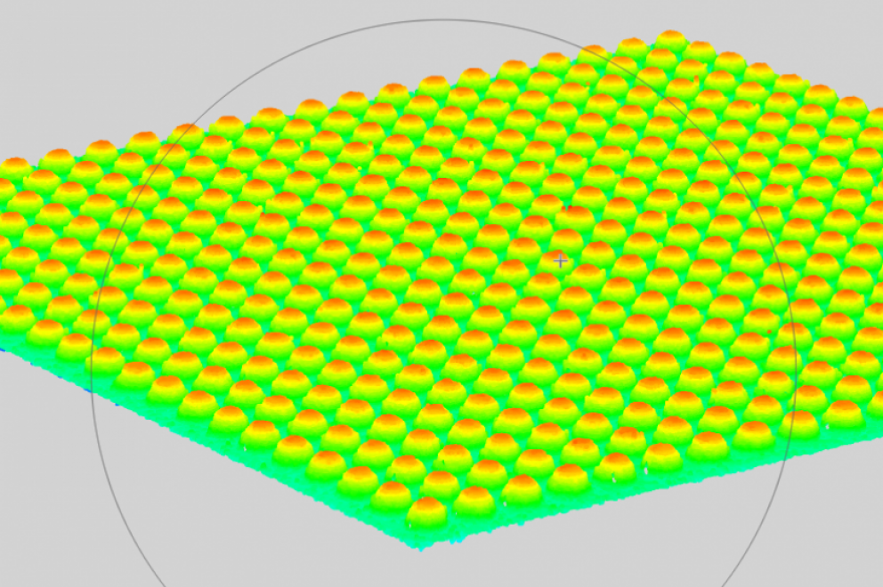
Height mark of a ball grid arrangement (BGA)
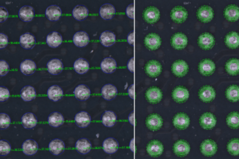
Position & size measurement of single solder balls
Chromasens is your ideal partner for configuring the perfect AOI system, thanks to its many years of experience in this application area. We can also provide you with a fully integrated vision system, from the camera to the optics and lighting, if desired.
For optimum image quality and stable error detection, lighting that is tailored to the application is absolutely essential. We offer coaxial and diffuse lighting especially for the semiconductor and electronics sector.
Different illumination geometries are used to detect as many defects as possible. Dust and dirt particles are made visible with dark-field illumination, scratches can be highlighted in the coaxial or bright-field geometry in the captured image. The optical inspection of freely formed, highly reflective components requires a diffuse, non-directional line illumination. The typically very high resolution of the camera systems requires high performance line illumination to achieve optimum image quality at high production rates.